PCB is a ubiquitous term in the electronic industry. Also known as the printed circuit board, these compact wiring boards made the tech revolution possible. The tech giants are now dreaming and working to bring the best within the most portable, eco-friendly devices. About a decade ago, this idea was mere science fiction. The magical intervention that made a dream come true is the invention of PCB. After several processes like PCB development, PCB manufacturing, and PCB testing come the final approach. The PCB fabrication and assembly. This last step makes the circuit board get loaded with our music, movie, or space analytical data. Before understanding the PCB fabrication process, it’s better to get a clear view of PCB development and testing processes.
Prior Steps of PCB Fabrication
PCB development is processing a design on a computer and setting for the prototype. Then it goes to the manufacturing stage. Here it develops the FR4 or the fiberglass core covered by copper wiring and soldering works. After that, the silkscreened cover makes the design good enough to work. But it has to pass the testing process. It’s also known as the bring up stage where all the backdrops and unwanted frequencies. After that, the assembly and fabrication stages come up. Please scroll below to know the steps of fabrication in detail. BTW, if you want to calculate PCB assembly cost in advance so that you could know the approximate budget, this could be a good piece of content to explore.
PCB Fabrication Manual
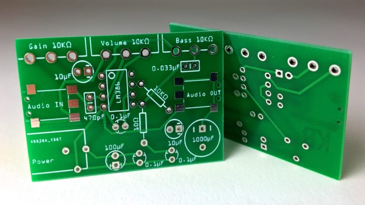
PCB fabrication means to bring all the layers of circuits together and give it a final, physical shape. The techniques include making a copper-clad laminate outlaying. Then you have to remove the extra copper pads or corners by etching. The most commonly and widely used etch material is ferric chloride. There are other techniques for this step too. Using an automated milling machine or printing the prototype is such. But they are either extremely expensive or not suitable for a time vs. production ratio. So. The ferric chloride remains on the top of the list. Stack up the layers by the heat and press method. However, there are chances of wrapping and malfunctioning, but till now, the best process to seal the thinner and finer sheets together to reduce the size while increasing the chip’s capacity. Mount the holes by chops and vias. This step is very crucial to maintain the proper transmission and compacting the activity. Plate the pinholes and via holes and finally cover the whole surface. Add the silkscreen to track the spots, polarization, indicators, brand logos, and any other customization you need on a special edition. Sometimes the professionals do an additional finishing to make it even better.
Importance of Knowing the PCB Fabrication
As an industrial engineer, buyer, or manufacturer, you need a clear idea of PCB fabrication. Because without this step, you won’t be able to put everything together and make it a visibly working structure. When you are a consultant, you will need prior knowledge to offer the best designs, sheet size, and thickness, affordability your company needs for the targeted audiences. The major throwback is manufacturing ability. Ensure the clearance of High Coefficient Of Thermal Expansion. Select the material according to the specifications. You can specify the boundaries of tolerance for your contact manufacturer to ensure there are no unused and unwanted sheets. This step will increase the effective yield rate. According to the quality controlling
Board, there are three acceptable classifications of PCB circuits. With the necessary knowledge, you make sure your PCB boards are up to the mark and satisfy your contact buyer’s need. Not only for reputation, but these steps are also directly related to consumer safety and tech development.